- 您现在的位置:买卖IC网 > Sheet目录333 > IRS21856SPBF (International Rectifier)IC DVR LOW SIDE/DUAL HI 14-SOIC
IRS21856S
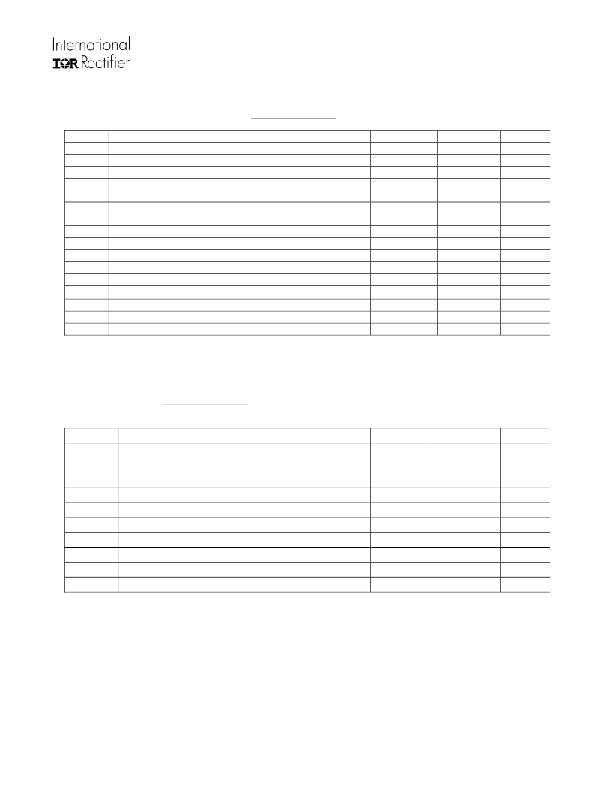
Absolute Maximum Ratings
Absolute maximum ratings indicate sustained limits beyond which damage to the device may occur. All
voltage parameters are absolute voltages referenced to COM .
Symbol Definition
Min
Max
Units
V CC
V IN
V LO
V DV ,
V VREF
V VSE ,
V RES
V B
V S
V HO1
Low side supply voltage
Logic input voltage (HIN1, HIN2, LIN3)
Low side gate drive output voltage
High side inputs voltage
High side inputs voltage
High side floating well supply voltage
High side floating well supply return voltage
Floating gate drive output voltage
-0.3
COM-0.3
COM-0.3
VS-0.3
VS-0.3
-0.3
VB-25
VS-0.3
25
VCC +0.3
VCC +0.3
VB+0.3
VB+0.3
625
VB+0.3
VB+0.3
V
V
V
V
V
V
V
V
dV S /dt Allowable VS offset supply transient relative to COM
-
50
V/ns
P D
R θ JA
T J
T S
T L
Package Power Dissipation @ TA<=+25oC
Thermal Resistance, Junction to Ambient
Junction Temperature
Storage Temperature
Lead temperature (Soldering, 10 seconds)
-
-
-55
-55
-
1.0
120
150
150
300
W
oC/W
oC
oC
oC
Recommended Operating Conditions
For proper operation, the device should be used within the recommended conditions. All voltage parameters
are absolute voltages referenced to COM . The offset rating are tested with supplies of (VCC-COM) = (VB-
VS)=15V.
Symbol
V CC
V IN
V LO3
V B
V RES
V DV
V VREF, VSE
V S
V HO1
T A
Definition
Low side supply voltage
HIN1, HIN2, LIN3 input voltage
Low side gate drive output voltage
High side floating well supply voltage
RES input voltage
DV input voltage
VREF and VSE input voltage
High side floating well supply offset voltage
Floating gate drive output voltage
Ambient Temperature
Min
10
COM
COM
V S +10
V S
V S
V S
Note2??
V S
-40
Max
20
V CC
V CC
V S +20
V B
V B
V B -3
600
V B
125
Units
V
V
V
V
V
V
V
V
V
oC
?
??
V S and V B voltages will be tolerant to short negative transient spikes. These will be defined and
specified in the future.
Logic operation for Vs of -5 to 600V. Logic state held for Vs of -5V to –V BS . (Please refer to Design Tip
DT97-3 for more details).
www.irf.com
8
? 2008 International Rectifier
发布紧急采购,3分钟左右您将得到回复。
相关PDF资料
IRS21858SPBF
IC DVR LOW SIDE/DUAL HI 16-SOIC
IRS21864STRPBF
IC DRIVER HI/LO SIDE 600V 14SOIC
IRS21867SPBF
IC MOSFET DRIVER
IRS21952SPBF
IC DVR HISIDE DUAL LOSIDE 16SOIC
IRS21953SPBF
IC DVR HISIDE DUAL LOSIDE 16SOIC
IRS21956SPBF
IC DVR HI SIDE/DUAL LOW 20-SOIC
IRS21962SPBF
IC DVR HI SIDE DUAL 600V 16-SOIC
IRS2301SPBF
IC DVR HI/LOW SIDE 600V 8-SOIC
相关代理商/技术参数
IRS21856STRPBF
功能描述:功率驱动器IC Ramp Slope Cntrl Driver Hi Volt RoHS:否 制造商:Micrel 产品:MOSFET Gate Drivers 类型:Low Cost High or Low Side MOSFET Driver 上升时间: 下降时间: 电源电压-最大:30 V 电源电压-最小:2.75 V 电源电流: 最大功率耗散: 最大工作温度:+ 85 C 安装风格:SMD/SMT 封装 / 箱体:SOIC-8 封装:Tube
IRS21858SPBF
功能描述:功率驱动器IC Hig Dual Side DRVR 600V 290mA 160ns RoHS:否 制造商:Micrel 产品:MOSFET Gate Drivers 类型:Low Cost High or Low Side MOSFET Driver 上升时间: 下降时间: 电源电压-最大:30 V 电源电压-最小:2.75 V 电源电流: 最大功率耗散: 最大工作温度:+ 85 C 安装风格:SMD/SMT 封装 / 箱体:SOIC-8 封装:Tube
IRS21858STRPBF
功能描述:功率驱动器IC Hi&Lw Sd Dual Drvr IC RoHS:否 制造商:Micrel 产品:MOSFET Gate Drivers 类型:Low Cost High or Low Side MOSFET Driver 上升时间: 下降时间: 电源电压-最大:30 V 电源电压-最小:2.75 V 电源电流: 最大功率耗散: 最大工作温度:+ 85 C 安装风格:SMD/SMT 封装 / 箱体:SOIC-8 封装:Tube
IRS2186
制造商:IRF 制造商全称:International Rectifier 功能描述:HIGH AND LOW SIDE DRIVER
IRS21864PBF
功能描述:功率驱动器IC Hi&Lw Sd Drvr capbl of 4A & 4A RoHS:否 制造商:Micrel 产品:MOSFET Gate Drivers 类型:Low Cost High or Low Side MOSFET Driver 上升时间: 下降时间: 电源电压-最大:30 V 电源电压-最小:2.75 V 电源电流: 最大功率耗散: 最大工作温度:+ 85 C 安装风格:SMD/SMT 封装 / 箱体:SOIC-8 封装:Tube
IRS21864PBF
制造商:International Rectifier 功能描述:MOSFET Driver IC
IRS21864SPbF
功能描述:功率驱动器IC HI LO SIDE DRVR 600V 10 to 20V 4A RoHS:否 制造商:Micrel 产品:MOSFET Gate Drivers 类型:Low Cost High or Low Side MOSFET Driver 上升时间: 下降时间: 电源电压-最大:30 V 电源电压-最小:2.75 V 电源电流: 最大功率耗散: 最大工作温度:+ 85 C 安装风格:SMD/SMT 封装 / 箱体:SOIC-8 封装:Tube
IRS21864SPBF
制造商:International Rectifier 功能描述:IC MOSFET DRIVER 制造商:International Rectifier 功能描述:IC, MOSFET DRIVER
